Processes

  • Metal Casting
    Metal Casting
    Processes
  • Resin Casting
    Resin Casting
    Processes
  • Reflow Soldering
    Reflow Soldering
    Processes
  • Circuit Design
    Circuit Design
    Processes
  • Polishing and Finishing
    Polishing and Finishing
    Processes
  • Loading Software
    Loading Software
    Processes
Sterling Silver Ring Cores.
3D Printed Casting Tree, Close Up.
Narrow Focus On Silver Casting.
3D Printed Casting Tree, Close Up.
3D Printed Casting Tree, Close up.
3D Printed Casting Tree, With Supports.
Metal Casting
The core of the ring is cast from precious metals. Currently silver, or gold. This metal core adds rigidity to the design to protect the internal electronics against flexing. The lustre of the silver or gold adds a classic design element that helps the world see this as a jewellery project rather than an electronic curiosity.The process is as follows:
  1. Design the items to be cast using CAD (Computer Aided Design) software, I am using AutoDesk Fusion 360.
  2. Arrange the items onto a casting tree in the CAD software. Care is taken to minimise the sharp corners and hard to reach areas (when the metal is cast into the final shape).
  3. Print the casting tree using a resin 3D printer. It is important to use casting specific resin, as it will perform better in the later steps.
  4. Place the 3D print into the casting flask and surround with investment casting material. Usually this is a gypsum based powder that is mixed with water, degassed, poured into the flask, then degassed/bubbled again.
  5. Place the casting flux in the burnout oven. This is an oven that follows a set heating program, around 14 hours of slowly ramping between the temperatures recommended by the investment material manufacturer.
  6. The metal to be cast is placed in the melt furnace and brought to its particular pouring temperature. (I use ~970c for silver)
  7. The flask is placed onto a vacuum table, which sucks air through the porous investment material. This will help the metal flow into all the details, and stop the expanding hot air from pushing out the metal.
  8. When the vacuum in the table is ready, the metal is pored into the flask.
  9. 15 minutes is allowed for the metal to solidify.
  10. The whole flask is dumped into cold water to break up the investment material.
  11. Finally! we have a metal version of the casting tree we designed in the CAD software. This process will usually take ~ 2 working days. ~10h for the 3D printing, ~14h for burnout. Total manual labour is about 2h, not including the item design time.
Categories :
Processes
Resin cast onto test PCB, sprues removed.
Resin cast onto test PCB.
Resin Casting

Resin casting is used to encapsulate the electronics, to keep them safe as well as providing a tactile, smooth outer surface. The resin is clear to allow light to charge the internal super capacitors, and to allow the time display to be visible.

The process I usually use is the following:

  1. The model to be cast is designed using CAD (Computer Aided Design) software. Care is taken to avoid features that are hard to cast, like very thin walls or points etc.
  2. The model is rigged with a cone and sprue, that will become the way that the resin is poured into the part. Extra sprues can be added to assist flow to hard to reach areas of the model.
  3. The model and sprues is attached to the bottom of an appropriately sized container.
  4. A 2 part silicone is mixed, then degassed in a vacuum chamber.
  5. The silicone is poured into the container.
  6. The whole container is placed in a vacuum chamber again, to help remove trapped bubbles.
  7. Optionally the whole container can be placed inside a pressure chamber to cure. (this means any remaining bubbles will be the same size when casting the resin).
  8. When the silicone is cured, it is cut open to remove the master model.
  9. The mould is then placed back inside its container to hold it closed.
  10. The resin is mixed, and degassed in a vacuum chamber.
  11. The resin is poured into the mould.
  12. The mould is again placed in the vacuum chamber to free all the air trapped in the bottom of the mould. When releasing the vacuum, lots of resin will be drawn deeply into the mould.
  13. The mould is placed in a pressure chamber to finally reduce the size of any remaining bubbles.
  14. The mould is removed from the pressure chamber and opened after curing (48hours or more)
  15. We now have a copy of the master!
  16. Remove the cone and sprues leaving the final part. Finishing and polishing is needed here to remove sprue connections etc.
Categories :
Processes
Main Electronics
Main Electronics
7 Segment Close Up.
7 Segment Close Up.
Reflow Soldering

Reflow soldering is the process of soldering using a paste comprised of flux and solder metal. Surface tension is used to move the parts to their final locations. This project has some particular challenges.

  1. Flex PCBs are sensitive to high temperatures. Minimum heating cycles and lower temperatures should be used when possible. Most components are placed with a low temperature solder paste. The solar panels are placed with no paste, only a layer of tacky flux, the solder balls on the bottom of the solar panels are used to connect them to the PCB.
  2. The use of small parts necessitates more than typical attention when placing parts. The clock crystal for example is a 0.9×0.6mm part with 4 BGA pins on the bottom!
  3. Special layouts, especially for the 7 segments, are used to allow parts to touch each other. Very non-standard, but required in this design. These parts will attract each other during reflow! This makes rework very difficult.
  4. The high density dual sided flex is very difficult to apply paste to. Only one side can be applied with a stencil, as the second side cannot be placed flat. Luckily only the LEDs on the top side need to use paste, as the solar panels use their own solder balls. Currently the LED paste is applied by hand with a syringe. Potentially a jig could be made to allow placing paste on the top side.

The current procedure is as follows:

  1. Paste is applied via a stencil on the reverse side, the side with the super caps and the majority of the circuitry.
  2. Parts are placed by hand using a vacuum pen (which is a custom Milwaukee battery compatible vacuum pen of my own design.)
  3. This side is reflowed using a hot air station.
  4. The PCB is flipped, and flux is applied to the solar panel region. This area is heated with hot air to allow the flux to flow to a thin layer. This allows the parts to stick to the PCB (as well as make the joints flow nicely)
  5. Solder paste is applied using a syringe to the LED section.
  6. All the parts are placed using the vacuum pen.
  7. This side is reflowed using the hot air station.
  8. The whole board is cleaned extensively with IPA. I cannot use ultrasound, as the crystal manufacturer forbids it.
  9. Fin.
Categories :
Processes
Circuit Design

This project has some unique challenges for circuit design.

  1. The aspect ratio of the PCB is very high, measuring 5mm x 65mm. This produces a bottleneck for signals to traverse the PCB
  2. The PCB must be flexible as it is wrapped around the metal core.
  3. The PCB is double sided, as all of the upper layer must be dedicated to collecting light and for the LED display.
  4. The small surface area necessitates a very high density, which is unusual for a flex PCB.
Categories :
Processes
Drill Internal Polishing Jig
Drill Polishing Jig External
Polishing and Finishing

When the PCB is potted into the metal core it must be machined down to its final dimension and then polished. Interestingly several of the components are partially located outside the final dimensions of the ring. This means that the machining step will remove parts of these devices. For example the LEDs making up the display are intended to intersect with the final polished surface of the ring. This is done to make the ring as thin as possible.

A big challenge for polishing is the fact that the final surface of the ring is resin. Currently this is an epoxy resin, though I will try polyurethane also. These can be as hard as 90-100 Shore D. This is enough to be polished to a high gloss. Though rings are notorious for getting scratched, even when using relatively hard metals. Being worn on the hand, they are constantly in contact with other hard surfaces, grit and other jewellery. This is still an open question, and will be a big factor in whether the product is viable for sale.

Categories :
Processes
Programming Jig Front
Programming Jig Front Close
Programming Jig Side
Loading Software

There are two software loading processes in this project:

    1. Direct programming:
      This is using the standard STM32 interface to program the microcontroller. This is done on the development boards where there are no robustness concerns for the input pins.
    2. Protected programming:
      When the ring is polished and finished, it should still be able to be programmed to account for final development and potential firmware fixes during deployment. However, on the final form factor all of the programming pins must be robust to external signals, including short circuits. Therefore some additional protection is added.


SignalProtectionDescription
3.322Ohms + forward biased diode.Resistor limits the inrush current to protect the diode. The diode is to stop charge from leaving the super capacitors via the charging pin. For example if the charging pin was shorted to ground, as is the case when using the auxiliary carry case button.
ResetSeries 62kOhm resistorCombined with the internal pullup, it is required to pull the pin to negative 3.3V to reset.
SWDIO/SWCLKSeries 1kOhm resistorLimits current if exposed to the negative reset voltage.


Categories :
Processes

Design Decisions

  • Energy Storage and Topology.
    Energy Storage and Topology.
    DesignDecisions
  • Display
    Display
    DesignDecisions
  • User Interface
    User Interface
    DesignDecisions
Energy Storage and Topology.

Energy storage is one of the most difficult problems to solve in this project, few applications have such tight volume, self discharge, burst current and longevity requirements. Throughout the development of the project there has been many twists and turns in the storage and topology. First I will outline the options for energy storage in this size class.

Energy Storage Type.RechargeableNominal VoltageDuplicates in Ring.CapacityLife time CapacityPeak CurrentForm FactorNotes
Silver Oxide 337No1.55V2-4~8mAh~8mAh> 10mA4.8mm Diameter 1.6mm thicknessRequires end user replacement.
ML414HYes3V2-41mAh300mAh20uA4.8mm Diameter 1.4mm thicknessMax current not enough for lighting LEDs.
CerachargeYes1.5V4-100.1mAh> 100mAh~1mA4.4 x 3.0 x 1.1mmA good option!
Super Capacitor CPH3225AYes3.3V10-200.011mF (4uAh)>300mAh10mA3.5 x 2.8 x 1mmBest longevity, easily supplies max current.


Replaceable Batteries

Initially the ring was designed to use the silver oxide batteries (Ring Version 1.0). These allow for a very simple design, as there is no need to recharge the batteries, they would last many months before needing to be replaced. However the need for the user to replace the batteries necessitates careful design of a very small water proof battery housing. This adds bulk and complexity.

User Charging

It is possible to combine different options to get the best of both worlds, for example the ML414 could be used for bulk energy storage, then the CPH3225A could be used to supply burst current for lighting the LEDs. However, the high energy density options like the ML414 have very poor cycle life. Assuming a charge cycle every few weeks, the ring would have a life span of only a few years before the battery no longer holds adequate charge. This also ends up complicating the circuit and using up lots of space.

The Ceracharge batteries are a good middle ground. With enough duplicates they can comfortably provide enough current, and their capacity is much greater than the super capacitor (CPH3225A), enough for about a couple of weeks of runtime. However, these have a similar lifecycle issue. The datasheet cannot guarantee useful lifespan beyond 10 years of usage.

Self Charging

Wanting to remove the user worry about maintaining adequate charge in the ring, I moved to designing self-charging designs. Even for energy storage options that have poor cycle life, self charging would allow the maximum degradation of the energy storage to be much worse before the ring is unusable.

The two reasonable options for energy harvesting are: Light, Thermal Gradients.

Thermal gradients seem like they could provide enough total energy to support this project. However, the physical size of the system would be hard to keep small. This is because there would have to be a “cold side”, likely a section of the ring with fins to dissipate heat. This would add unacceptable bulk for the sleek design intensions for this project. (It is an interesting enough idea that I am pursuing it separately though!)

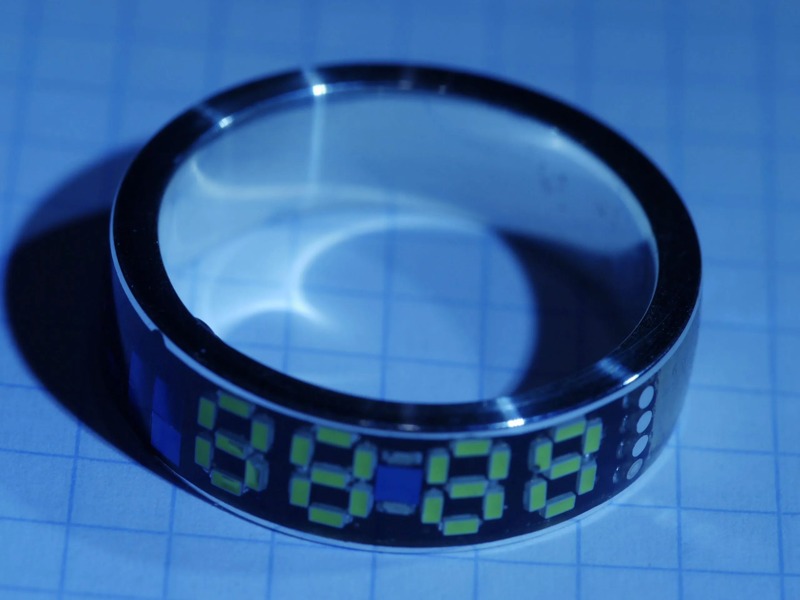
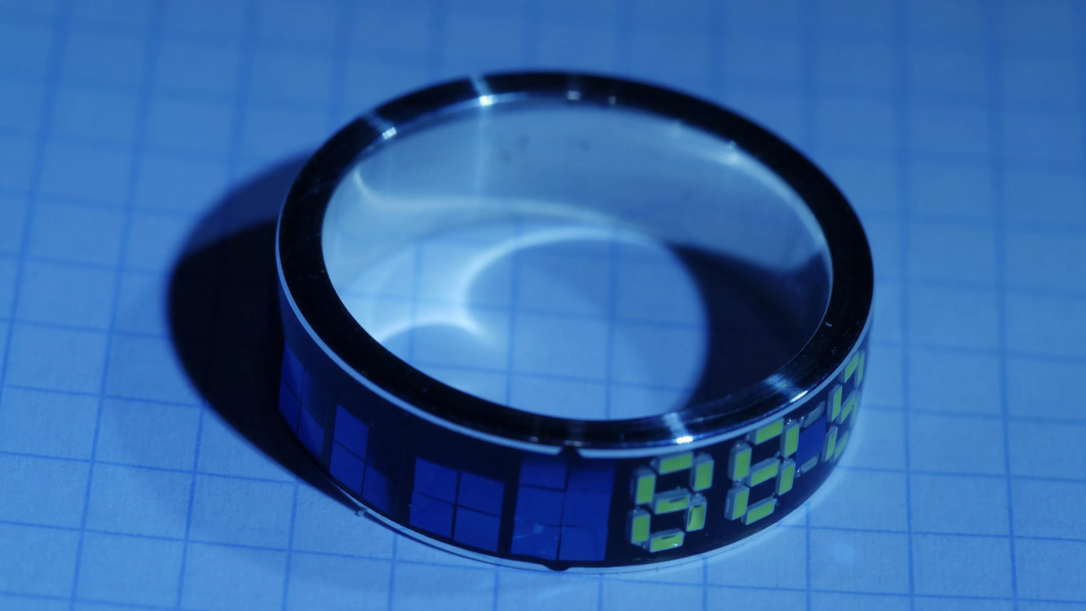
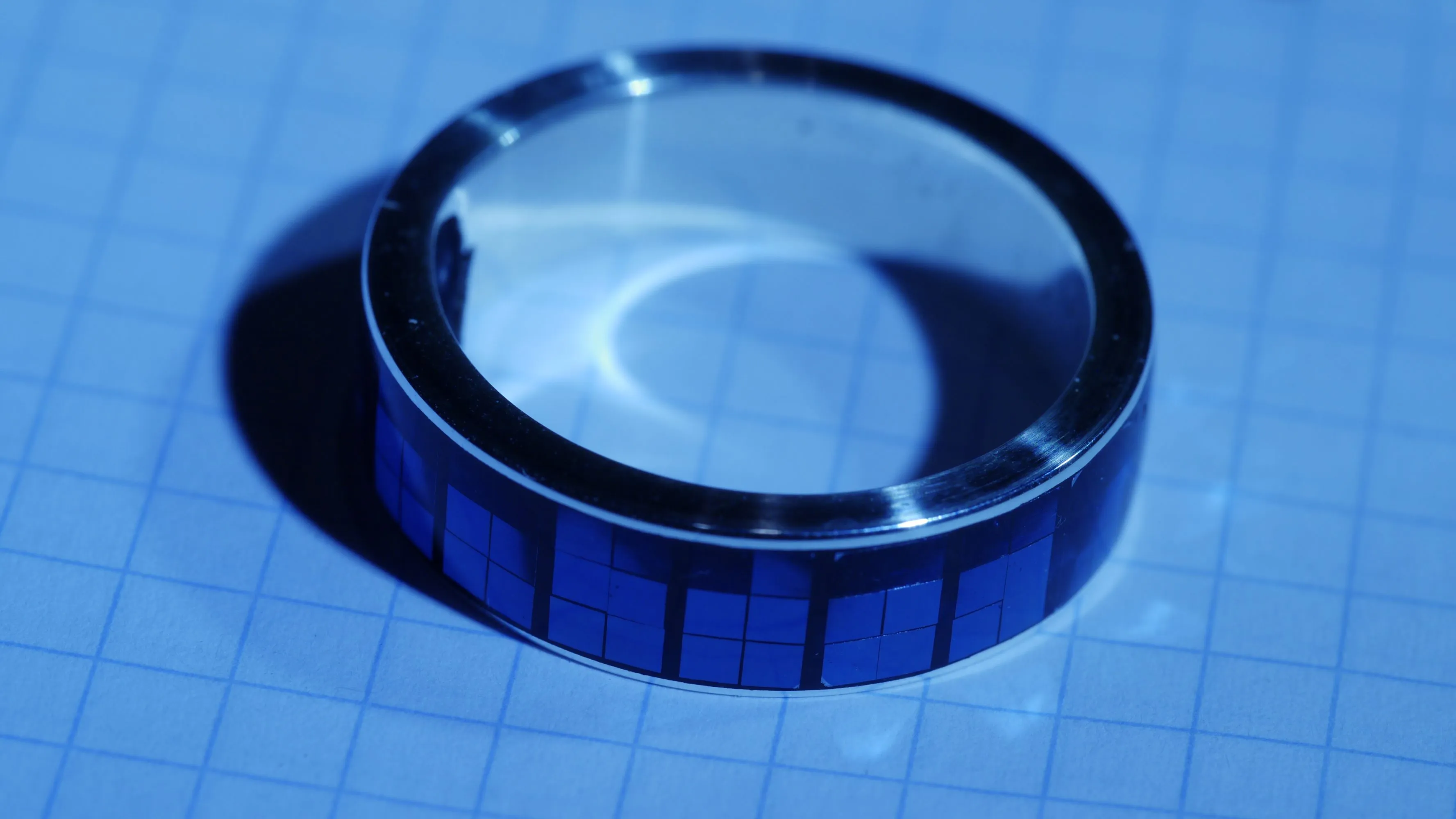
Light / Solar is the other good option. This allows for a very compact design, as solar cells can be made thin. An additional benefit is that it is easy to make a series array of arbitrary voltage, which simplifies the harvesting electronics. The main downside however is that there is not very much surface area and light intensity to work with. My calculations suggest that it is marginal that the ring could survive in a well lit room. This would still allow the energy storage to “coast” for longer. This is despite the circuitry for harvesting displacing about 25% of the space that could be used for more storage.

However, if the user goes outside even for a few minutes a day, the whole calculation becomes much more favourable. Even an overcast day is typically 50-100 times brighter than inside.

Charging Circuits

Charging CircuitMPPT MethodQuiescent current in mild light.Efficiency in low light.Efficiency In Bright Light
bq25504Fixed ratio of open circuit voltage.1-2uABadVery Good
LDO based.Fixed by absolute value based on storage element voltage.< 100nAGoodVery Bad
R1800KFixed by absolute value based on R1800K SKU.144nAGoodGood

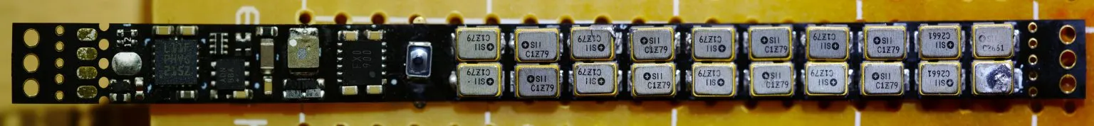
I initially used the bq25504, I was drawn in by its low quiescent current values. Later I discovered this was misleading, as these are quoted when in shutdown (due to a full storage element etc), however it is significantly more when the converter is actively trying to extract energy, it seems to be about 15uA in that case.

This issue led me to thinking about a very low quiescent current method, even when energy is being actively extracted. If the photodiode string is fed directly into a LDO, which then charges the storage element through a diode, the quiescent current can be very low. The power point tracking would be done very naively, where the photodiode string length would be matched to the storage element voltage such that the system is near its maximum power point in “normal” conditions. If this was calibrated for typical indoors lighting efficiency could be quite good. The poor efficiency when in very bright light is usually less important, as in that situation you are likely to have enough energy to fairly quickly saturate the storage element.

I then found the R1800k series of chips. This is basically a switch mode version of the above. The “maximum” power point is set to a fixed voltage via selecting a specific chip SKU. Again you would specify this for your “normal” operating conditions. The fact that is is a buck regulator allows somewhat independent selection of the photodiode string voltage and storage element nominal voltage. Whenever the input voltage rises above the MPP, the converter moves the energy to the output, until the terminal charge voltage is reached. The chip is then deactivated, allowing the input voltage to rise to the photodiode string open circuit voltage. This chip has a very low quiesent current of only 144nA, it uses more than this while switching, though it will not switch often in very low light, limiting the practical amount of energy it wastes. This chip will break even at 720nW, compared to the bq25504 at around 15uW, which in this application where there is typically ~3uW available in normal indoor lighting is quite an important difference.

Categories :
DesignDecisions
Display

There were two primary options that were considered: E-ink, 7 Segment LEDs. Both have their allures!

E-ink

There are E-ink modules that are small enough and flexible that could potentially be put into the ring design. However, these were primarily designed for low cost products like smart cards with embedded counter displays. Hence the available ones do not sleek enough to put in a jewellery design. Power is also a consideration. On the upside these displays use no power at all when static, allowing the time to be displayed constantly without the user needing to trigger it. The downside however is that the display must then be updated every minute to allow the displayed time to remain correct, even if the user is not looking at the display in that time. Updating the E-ink displays is fairly energy intensive, requiring a large voltage which is challenging to generate in a compact circuit. Overall this means that the power draw of this display type is prohibitive.

A particular advantage of this type of display is that there is no upper limit to the ambiant light it can be viewed in, even direct sunlight it should remain clear. However, the opposite is not true, when it is dark the display will not be visible.

7 Segment LEDs

When using a set of normal LEDs in a 7 segment arrangement, no power is needed to update the display each minute when the user is not looking. Simply a blank display is presented. To view the time the user would have to activate the display with a button press (or similar). This means that the baseline power draw is zero for this display type.

Unfortunately the current needed to light the display when being viewed can be quite large. In typical indoor lighting it is usually around 1mA. Outdoors it is as much as 30-40mA. These current values are the aggregate across the display. The current is shared across all the LEDs via time domain multiplexing. Luckily, as the current design is solar powered, we can assume that we are also harvesting large amounts of energy when outdoors, hopefully recuperating this large current outlay.

While with adequate current the display should be visible in outdoors lighting, direct sunlight is likely to be an issue. However, in very low light the display will still be visible. This is the opposite trade-off to the E-ink dis

The Verdict

In the current design I have chosen to use the 7 Segment LED displays. This is because I anticipate that the viewing time of the display will be only a few seconds per hour, and that the energy use of the display correlates with the available energy harvesting from ambient light. (High currents are needed when bright light is available to offset it, display current is very low when in darkness, no updates are needed while the user is sleeping!). Further I believe that the aesthetics of the display are pleasing, and suite the jewellery design ambitions.

Categories :
DesignDecisions
User Interface

Because the LED display uses lots of power to display the time, the user must indicate to the system that they are ready to view the time. I have experimented with 3 different options.

Interface MethodCurrent UsageAdvantageDisadvantage
IMU270nANo exterior to waterproof.Gestures are clunky.
Resistive Contact>30uAEasy to waterproof, looks sleekFloating mcu inputs use lots of current!
Tactile Button.< 100nALowest Power, satisfying clickComplicated to waterproof.

The table above is the order in which I implemented them.

IMU

The allure of an easy to waterproof and low power solution drew me to the adxl362 by Analog Devices. Though in order to use its lowest power mode you only get a 6hz measurement, and are provided with an interrupt when the acceleration changes by a set amount. This only enables a very clunky gesture of triggering the magnitude threshold with some particular timing. This was difficult to trigger reliably, though it would also trigger accidentally, wasting current on the LEDs when no one was looking.

Resistive Contact

Next I moved on to a floating input to the MCU exposed on the outside of the ring, this could then be pulled low through the users skin to an adjacent ground connection. I used a large external pullup in the 1Mohm range, which could be pulled to ground through the ~100kOhm resistance of the skin over a short distance. This worked well, and had the advantage that the external contacts contained no moving parts, making it easy to waterproof. Unfortunately sometimes the users skin is too dry, and will fail to trigger the button without excessive pressure applied to get a good contact. Though due to the entirely rigid nature of the system there was no tactile feedback to the user, making it pretty unsatisfying to use. The killer however is the surprisingly high current draw. My initial thought was that the current draw would be small, as usually the MCU input is open circuit, even when shorted, it would be through a 1Mohm resistor. However, in practice allowing an MCU input to float halfway in its voltage range causes significant leakage, in the 10uA+ range. You could use the pin in analog mode, though then the ADC sampling and thresholding would use a similar amount of current.

Tactile Button

The current solution is to use a tactile momentary switch. Specifically the NANOT240AS by C&K. This button is on of the thinnest IP67 rated momentary switch that can be used in this application. A secondary waterproofing O-ring and plunger needs to be engineered into the metal core of the V3.0 ring to allow the user to press it, and avoid water being trapped beneath the plunger. In the current incarnation the button is on the inside of the ring, and the user presses the whole ring against their finger to activate it. This is nice as it allows a good degree of leeway in the pressing action, also it allows the top surface of the ring to be dedicated to collecting energy and displaying the time.

Categories :
DesignDecisions

Analysis

  • Cost Analysis
    Cost Analysis
    Analysis
  • Power Analysis
    Power Analysis
    Analysis
Cost Analysis

Electronics Cost

The cost of the project will constantly be changing as parts themselves  fluctuate, must be replaced due to obsolescence etc. This has happened many times over the time since 2018 when I started on this project. The below estimate can provide a rough estimate using 2023 prices. Not included is the cost of the PCBs, currently I get about 50 duplicates for 200USD, these would be nearly free at large quantities. They are not included below as they distort the QTY 1 in an unreasonable way as they are more reasonable thought of as a fixed cost at this quantity.

This table represents the cost for the electronic components. They are price both when purchasing for 1 finished ring and for 100 finished rings.

ComponentQtyPrice (QTY 1)Price (QTY 100)Line Cost (1 QTY)Line Cost (100 QTY) 
Super Capacitor201.570.79831.415.96
PhotoDiodes670.780.5952.2639.53
7 Seg LEDs280.2580.097.2242.52
Dot LED20.420.150.840.3
Crystal11.581.281.581.28
MCU13.092.233.092.23
Boost IC12.832.052.832.05
Harvest IC14.042.984.042.98
button10.730.5880.730.588
diode50.30.0851.50.425
Inductor Harvest12.041.352.041.35
Inductor Boost10.390.2150.390.215
Swdio Resistor10.110.0390.110.039
LED Resistor 410.160.0970.160.097
LED Resistor 210.130.0390.130.039
Charge Resistor10.110.0380.110.038
Reset Resistor10.10.0080.10.008
EnablePullUp10.10.0170.10.017
Voltage Set10.10.0080.10.008
Harvest In Caps20.110.0410.220.082
HarvestCapsOut, Other60.170.041.020.24
reset capacitor10.10.0110.10.011
Total:110.07470.007


Metal Cost

The inner core is made of precious metal. Below is an estimate of the cost of the core. This is assuming zero waste, recycling sprues etc. This shows that silver is a reasonable price while being a metal popularly understood to be “Jewellery Grade”. Versions made from gold should be no more difficult to construct, though the cost is significant. Most of the metals can be mixed with second hand material from previous runs at a maximum rate of about 50% new : 50% old. For efficient reuse of sprue material it would be important to have the final product take > 50% of the volume of the casting tree. (difficult with such thin inner cores). I would need about 10cc of metal to fill sprues etc, which is a significant cost if using gold.

MetalDensity g/ccgrams needed Price $/gCost $
Silver10.33.810.72.67
gold 9k114.0723.4995.60
gold 18k15.45.7046.98267.69


Labour Cost

The labour involved in producing this ring is likely the biggest factor in its viability. Unlike most electronics project, even at medium scale it must be made by hand, even PCB pick and place is unlikely to be viable to automate. Below is a very rough estimate of the time taken for each process. Note that the metal casting steps can produce multiple rings in parallel with little extra effort, all other processes are done per ring. Attaching a dollar value to this time is difficult. I personally do this as a hobby, which is fine while making one or two, and I have all the skills and experience to produce the ring in one place, employing such a person is not normally free! You can see that the time taken is about 1 working day per ring, feel free to estimate this cost as you feel is appropriate. Perhaps with pipelining, process improvements, we could estimate 2 rings per day per worker is possible when producing > 500 rings a year.

OperationMan HoursRings ProducedPer Ring Time
Fixture PCB, Stencil0.2510.25
Place Rear Parts0.7510.75
Manual Paste Top0.2510.25
Place Top parts0.7510.75
QC Circuit Function0.510.5
Solder Prog Pins0.110.1
Electronics Total2.612.6
Print Casting Tree0.2560.0416
Print Clean Up0.560.0833
Cast Investment0.560.0833
Setup Casting0.560.0833
Pour and Cleanup0.7560.125
Removing Parts160.166
Metal Core Total3.560.583
Glue PCB0.510.5
Cleaning0.510.5
Setup Epoxy Cast0.510.5
Epoxy Casting0.2510.25
Serparating parts0.510.5
Dimension reduction111
Polishing111
Assembly Total4.2514.25
Ring Production Total7.433


Equipment

It is difficult to appropriately assign the cost of equipment to the project when working on a hobby basis. In general the equipment I use is of modest quality, appropriate for non-professional use. This set of hobby-level equipment costs in the region of $2000, if I was making >100 rings per year, more appropriate equipment would represent an outlay of ~$10,000. Estimating other fixed costs will be left as an exercise for the reader, > 100 rings per year would be a small business, and have the associate miscellaneous costs (Workshop space, Legal, HR, Accounting etc).


Cost Of Goods Sold

Adding in some extra lines without too much justification we can estimate the COGS (Cost of Goods Sold).

Line ItemCost Per Ring (Silver, QTY 1)Cost Per Ring (Silver, QTY 100)Cost Per Ring (Gold 18k, QTY 1)Cost Per Ring (Gold 18k, QTY 100)
Electronics110.0770.00110.0770.0
Metal Core (Silver)2.662.66267.69267.69
Labour (50USD/h)371.66185.83371.66185.83
Charging Box155155
Postage50505050
Total549.40313.50814.43578.53

Price To Market

(This is all hypothetical, currently I have no intention to sell these rings)

The final sale price of such a ring would depend on the goals of the business. If this is a cottage industry/hobby, perhaps the margins are capably of being thinner, essentially operating as a justification for getting nice tools. However for a product to be viable it should be sold for at least 2x of the COGS price. This is to account for the supply chain, advertising, returns, damage, waste etc. Ideally a high risk product like this would have a multiplier of >3. Failure of the electronics, gold wasted into broken product (recycling is more difficult with epoxy casted/electronics laden gold), returns based on customer taste or incorrect sizing are all factors that would increase risk over a typical electronics project.

Therefore it is hard to imagine that the current design could be sold for much less than about $1000 USD, or more for a gold version. Reduction of the labour price is the lowest hanging fruit, perhaps pipelining operations into many simpler jobs would allow the use of less skilled people. Though this would always be a luxury product, as such craftsmanship and attention to detail are a must, so retaining any employees would be critical to developing all the skills necessary to reach the target quality.

Categories :
Analysis
Power Analysis

Fundamentally this project is an exercise in low power electronics wrapped up to look like jewellery. In efforts to reduce fiddly battery changing and the inevitable “I will get around to it” followed by the ring never being worn again version 2 and 3 are powered by solar/ambient light. This choice puts a hard limit on the amount of power that the ring is allowed to use. In the case of replaceable batteries a heavy user of the ring could just replace the batteries more frequently, though that user is unlikely to spend more time outside just to give the ring more power!

Therefore we should have an understanding of how much energy the ring will use in a typical day, and how much it would generate.

LED Power

By far the highest current draw in the system is lighting the LEDs. This ranges from 100uA in a dark room, to 12mA in direct sunlight. Typical indoor usage is estimated to be about 3mA to give a legible display.

If we estimate that the user will look at the display for 1 second every 30 minutes for 16 hours a day, a reasonable estimate of the LED power use is: 3mA*3.3V*(32s/(24*3600)s = 3.66uW, or 0.317J per day.

Standby Power

We can estimate the standby power by looking at the data sheets for the current draw for all relevant components. A rough table is provided below:

ComponentCurrent nANotes
Harvest Chip144
Boost Chip128.595% 30nA 5% 2uA
Super Capacitors500This has complicated dependencies.
MCU + RTC600
Reverse Leakage Diode28Worst case.
MCU (intermitant)30Book keeping every ~5min
Total1430.5
Power (@3.3V) W4.72065E-06
Energy per day (J)0.40786416

Generated Power

The power generated from harvesting light will depend strongly on the user’s habits, going outside is hugely valuable! Lets make the following assumptions about their day:

ConditionTimePower Generated uWGenerated Energy J
Overcast Daylight0.53000.54
Inside (daytime)870.2016
Inside (evening/morning)820.0576
Sleep7.500
Total240.7992

These values are hard to justify, as calculating values from data sheets is possible, though the fudge factors end up dominating. Examples of these fudge factors: shading of the solar panels by the hand, wavelengths available in the indoor lighting, brightness of the day etc. A flat array in direct sun can generate ~6mW, this could provide the 0.7J required in 2 minutes! Though account for the array being round, and indirect sunlight, you can see that perhaps a factor of 15 seems reasonable, or about 30minutes outside.

A flat array also has been measured to be self sustaining in a standard office lighting condition (200lux LED lighting), the roundness of the array would be less of a disadvantage in this ambient lighting condition. Consequently my estimates is that the ring will generate no power in the dark, will glide downwards in residential lighting, will break even in working lighting and be very profitable when outdoors.

Categories :
Analysis

Todo: Power Budget Calculations, Cost estimates. Product Feasibility.

Versions

  • Version 1
    Version 1
    Versions
  • Version 2
    Version 2
    Versions
  • Version 3
    Version 3
    Versions
Version 1

This version has the following features:

  1. User replacable silver oxide batteries, 2x 1.55V 8mAh.
  2. Attempts were made at an O-ring seal for the battery compartment.
  3. The display was activated with a gesture detected by an IMU.
  4. The time was displayed on the top, near the knuckles.
  5. It could be worn on any finger, as it did not rely on physical buttons.
  6. It was programmed before casting, and there was no way to modify the code.
Categories :
Versions
Version 2, Render, Solar Panels.
Version 2, Render, LEDs, ISO
Assembly_narrow_2020-Apr-16_09-24-37PM-000_CustomizedView12686642520
Assembly_narrow_2020-Apr-16_09-18-46PM-000_CustomizedView21703375907
Version 2

This version only made it do the development board phase. Hence the images here are all renders. This version featured the following:

  1. The ring is now charge via ambient light using 4 large photodiodes.
  2. The display is moved to the palm side of the ring, to allow the photodiodes to point outwards.
  3. The ring is activated with a resistive contact “button”. When the user connects the two gold contacts using their thumb, the GPIO is pulled low, activating the display. This method has no moving parts, and looks great!
  4. The PCB still only has parts on one side.
  5. The power storage element is 4 CeraCharge batteries, 1.5v 0.1mAh, with a 2 serial 2 parallel connection.
  6. The ring can be reprogrammed using pins exposed on the final form factor.

These features led to the following issues with the design.

  1. The batteries give 3v with 0.2mAh, which is good, though the maximum current would be ~3 or 4mA. This would be OK for indoor use, but not outdoors.
  2. There was no space for a boost regulator, meaning the brightness of the LEDs would be hard to control, and would sag with the battery voltage, particularly under load.
  3. The total surface area of the photodiodes was limited by the requirement of having the board with parts on one side. Meaning the batteries and other components are using up outward-facing real-estate.
  4. The BQ5504 used for energy harvesting would only be effective in direct sunlight with such a small photodiode area. The rest of the time the small amount of power available do just enough to keep the converter awake (which wastes more power than it can generate!). For indoor use the converter actively wastes power. This chip also uses lots of board area due to the passives that it needs.
  5. The (nearly) floating GPIO ends up using lots of power (~30-100uA) if it is held in the middle of the voltage levels, which happens often if the pullup is weak enough to allow the thumb resistance to pull it down.
Categories :
Versions
Version 3, No Resin, Solar Panels.
Version 3, No Resin, Inside.
Version 3

Version 3 is the current version of the project. It has the following features:

  1. Very large surface area dedicated to solar panels (Photodiodes). They are arranged in 4 separate series strings allowing partial shading without loosing output from the other strings. This also allows a relatively high open circuit voltage, which can make harvesting more efficient.
  2. Super capacitor energy storage. 20x 11mF 3.3V. This is about an 1/3rd the energy as the ceracharge powered version 2. Though the lifespan of the capacitors should be much more. Also the max current of this system is > 100mA. This is no longer the limiting factor in making direct sunlight visible LEDs. (That is the current output of the GPIOs at 12mA.)
  3. Dual SMPS, one buck converter to take variable input from the solar panels and charge the super capacitors to 3.3V. A second one takes the variable voltage on the super capacitors and provides the MCU with 3.3V when the LEDs need to be lit. This boost SMPS can be turned off to allow the MCU to coast on a single 11mF super capacitor. This allows the average voltage supplied to the MCU to be lower, lowering the leakage current. It also removes the active quiescent current of the boost converter (~1uA). This is turned back on when the display needs to be lit, or if the voltage on the coast capacitor falls below a certain value. This is checked every 5 minutes.
  4. A sense photodiode is added to the display side of the ring. This allows the display brightness to be matched to the ambient lighting conditions.
  5. The programming pins are moved to the face of the ring. This allows the metal core to be a U-shaped channel all the way around, adding strength.
  6. The user now activates the display with a press of a button that is facing towards the finger the ring is worn on. The whole ring is pressed against the finger using the thumb to press the button. This frees up additional space on the top surface for more solar panels. Also this uses a trivial amount of current.
  7. The R1800K energy harvesting chip has a break even energy of 720nW, down from around 15uW for the previous design. This lets the harvester contribute even when in dimly lit rooms, helping the coast down in these conditions. It is still efficient enough in bright light to make the whole energy system self sustaining with ~20 minutes outside every 3 days.
  8. The programming pins can be used to charge the ring in its storage box, to allow long term storage without losing the time. Or for topping up if the user is aware they have been in the dark for too long.
  9. The programming pins can act as an additional input that can be activated by a press button in the charging box. This additional button is used to aid in the programming of the time for the end user.
Categories :
Versions